3-dimensional wafer-level-packaging (WLP) is the most suitable for miniaturizing semiconductor devices. It also can improve the high-frequency properties of the devices with the metal via.
Features
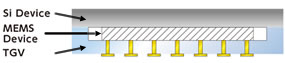
Through glass via makes it possible to minimize devices
● Anodic bonding with a silicon wafer is available Non-adhesive process can solve the out-gas issue ● Excellent high-frequency properties, ideal for RF application ・Low stray capacitance compared with TSV ・Low inductance ・Low electric-resistance (due to metal rods)
Suitable for WL-CSP MEMS packaging
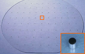
● Fine via pitch tolerance ・Consecutive pitch <±20μm/φ200 mm wafer ・Consecutive Via pitch <±20μm ● Available up to φ200mm wafers
Standard specifications
Material
Borofloat 33, SW-YY
Glass size
≦φ200mm
Min. thickness
0.3mm
Min. Via diameter
φ0.15mm
Hole size tolerance
±0.02mm
Max. aspect ratio
1 : 5
Via material
Si、W(Tungsten)
Via hermeticity ( He leak test )
1×10⁻⁹ Pa・m3/s
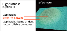
Via-Glass gap
Std.
0μm〜3.0μm
Option 1
0μm〜1.0μm
Option 2
-3.0μm〜0μm
Via shape
Straight
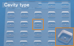
Cavity process
Available
Metallization process
Available
Bump process
Available
Note: These are standard specifications. In case you have any request for other than the above, please feel free to contact us.
TGV application sample
End user market / Applications
AV/Mobile
・ RF-switches/relays for mobile devices such as smartphones, portable video games, digital cameras, car navigation systems, Pressure sensors, Gyroscopes, Acceleration sensors, image sensors